


Hardware Design & PCB Development Services for US, Australian, and European Companies
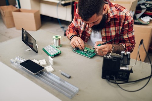
We are a globally recognized hardware design company delivering professional engineering solutions. Our market focuses on the USA, United Kingdom, Germany, Canada, Australia, Sweden, Switzerland, Denmark, the Netherlands, and across Europe. If you are searching for one of the best hardware design companies to accelerate your success, our expert team is ready to deliver. We offer full product development: hardware design (schematics, PCB layout), firmware, mechanical design, and a mobile app.
ContactHardware Design Services for High-Performance Electronic Products
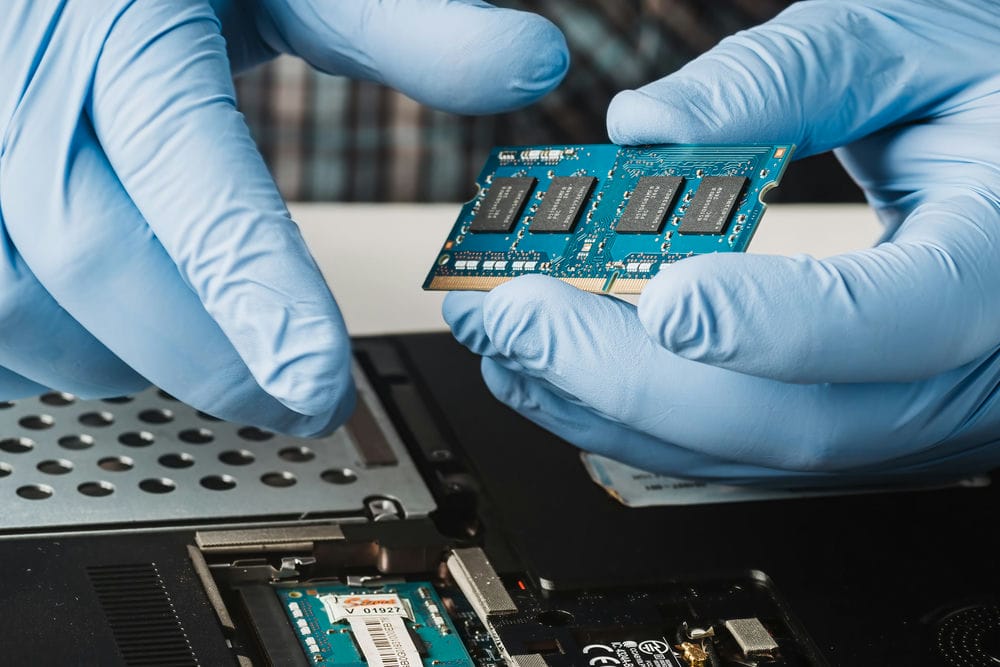
At Droid Technologies, we combine creativity, engineering precision, and industry expertise to deliver world-class hardware design services. We are among the best hardware design companies in Europe, trusted by clients from the USA, Germany, and across the world to transform their product concepts into certified, market-ready devices. Our engineers provide the complete hardware development cycle — from concept creation and schematic design to custom PCB design, simulation, prototyping, and pre-certification testing. We work with analog, digital, mixed-signal, and high-speed PCB layouts, ensuring every design meets EMC, CE, and FCC requirements and passes manufacturing validation.
Unlike many hardware design companies, Droid Technologies unites hardware, firmware, and mechanical design expertise under one roof. This allows us to optimize performance, reduce the BOM cost by up to 25%, and shorten development cycles by 30–40%. As a full-cycle custom PCB design company, we develop solutions for: - IoT and smart home electronics - Industrial control and automation - Medical and wearable devices - Automotive and mobility systems
Every design is backed by detailed documentation, DFM/DFT validation, and comprehensive design reviews that guarantee reliability, safety, and manufacturability. Each hardware design project goes through electrical, thermal, and mechanical verification, ensuring stable operation and full compliance with EMC, CE, and FCC requirements. Our approach ensures that every custom PCB design we deliver is not only functional but also optimized for mass production and long-term maintainability. We work closely with trusted manufacturing partners, providing PCB fabrication files, assembly drawings, and test procedures, so clients can seamlessly move from prototype to production. Following strict ISO 9001:2015 and ISO 13485 quality standards, we combine hardware design services, firmware integration, and mechanical engineering in a single workflow that minimizes risks and accelerates certification. This integrated process makes Droid Technologies a reliable partner for startups and established enterprises looking for end-to-end hardware design companies that deliver measurable results. Whether you are developing a new device from scratch or upgrading an existing product, our team ensures engineering excellence, transparency, and consistent performance at every stage — from concept and schematic capture to validation and PCB manufacturing support. Partner with one of the top hardware design companies in Europe and discover the difference of working with experts who truly understand electronics from idea to certification.
Hardware Design & PCB Development Capabilities
Custom Power Electronics Design
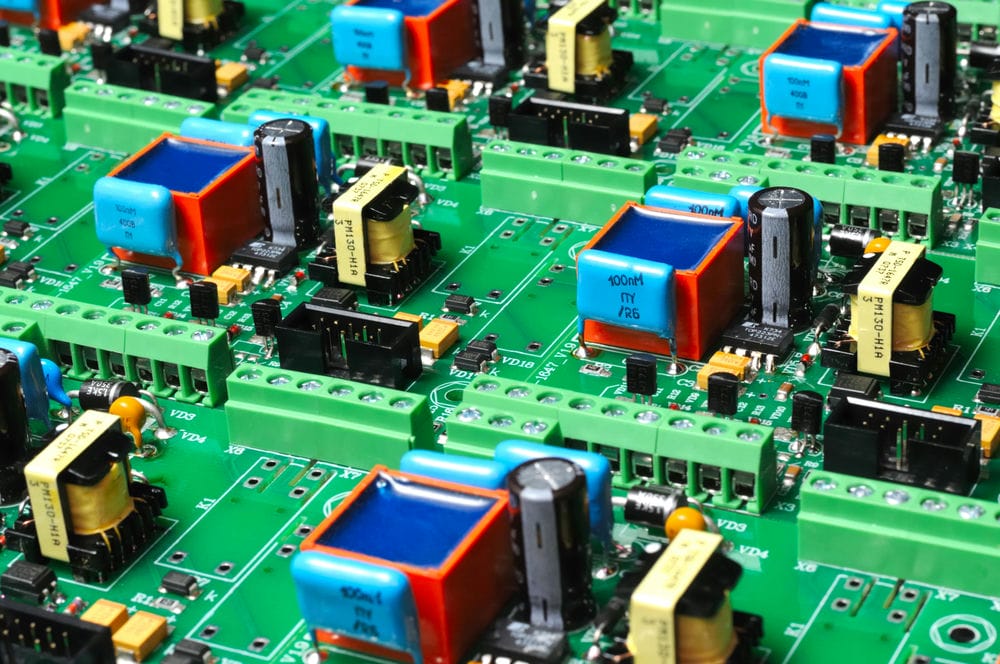
⚙️ Power Factor Correction (PFC) Design Droid Technologies — a professional hardware design company specializing in custom power electronics design. We design and optimize active and passive PFC circuits for high-efficiency power supplies, ensuring EMI/EMC compliance and global certifications (CE, FCC, UL). Our hardware and PCB design services improve power quality, reduce harmonics, and ensure reliability for industrial, automotive, and consumer applications. ⚙️ Solar Charging Controllers Design We develop custom solar charging controllers for PV systems, integrating MPPT algorithms, BMS, and communication interfaces (CAN, RS485, Modbus, BLE, Wi-Fi, LoRa). Our power electronics PCB design services cover both residential and industrial energy storage, combining hardware design expertise with efficient firmware control. ⚙️ Battery Chargers and Power Supplies As a top hardware design company, we create AC/DC and DC/DC chargers for Li-Ion, LiFePO₄, and lead-acid batteries. Our custom PCB design ensures optimal thermal management, safety protection, and high-efficiency conversion for reliable operation in the field. ⚙️ High-Voltage Control Systems We design precise, safe high-voltage circuits for automation, EV charging, and laboratory equipment. Our power electronics design engineers focus on isolation design, high-speed gate drivers, and galvanic isolation for stable operation under extreme voltage conditions. ⚙️ Motor Controllers (DC, AC, BLDC, PMSM) Our team develops custom motor control solutions — DC, AC, BLDC, and PMSM — integrating PFC stages, FOC, PWM, and sensorless control. We handle the power stage design (MOSFET/IGBT), firmware, and custom PCB layout, providing complete hardware design services for EVs, robotics, and industrial drives.
Analog electronics design
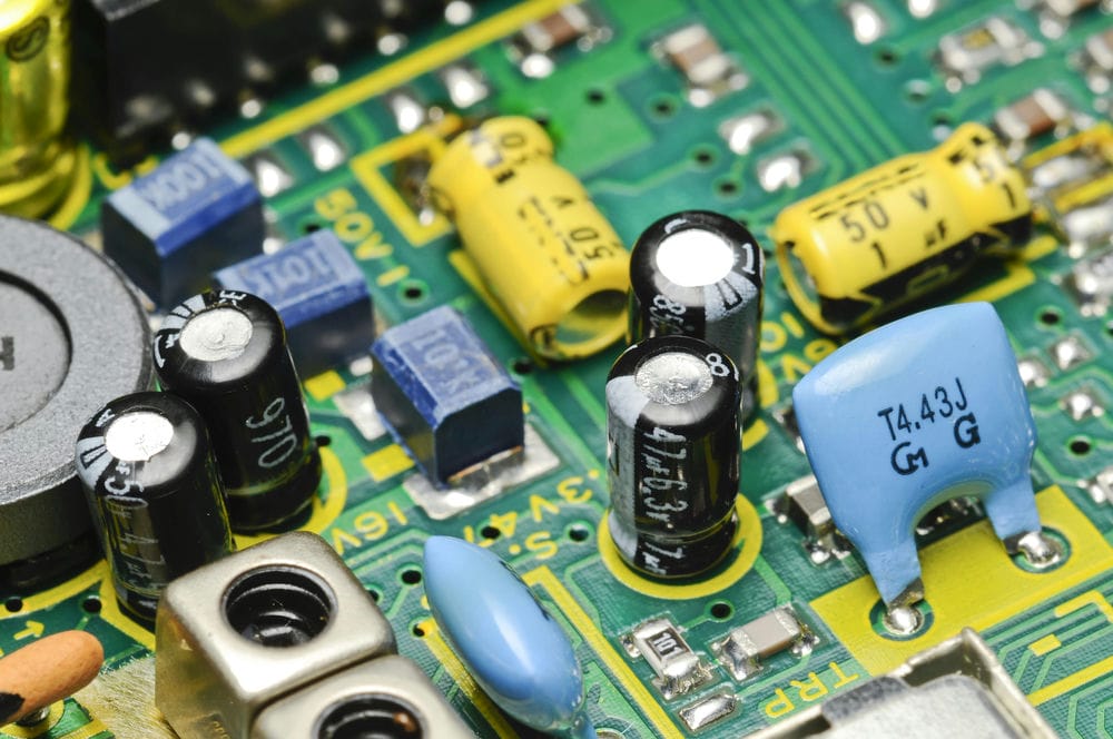
⚙️ High-Accuracy Analog Measurements As a professional hardware design company, Droid Technologies provides custom analog electronics design for precise signal acquisition — EEG, ECG, PPG, EMG, and piezo sensors. Our high-accuracy analog measurement circuits offer low noise, high input impedance, and optimized CMRR, ideal for medical devices, biosignal recorders, and wearables. ⚙️ Noise Filtration and Signal Conditioning Our analog electronics design services include advanced noise filtration using active RC, Sallen-Key, and Butterworth filters. Through custom PCB layout optimization, component selection, and ground isolation, we achieve excellent signal-to-noise ratio (SNR) for sensitive analog systems. ⚙️ Digital-to-Analog / Analog-to-Digital Conversion We integrate high-precision DACs and ADCs as part of our custom analog PCB design services. Our engineers ensure calibration, reference stability, and sampling synchronization for reliable and clean data conversion in embedded devices. ⚙️ Signal Amplification Droid Technologies develops analog signal amplification circuits with low-noise and instrumentation amplifiers. Our custom analog electronics maintain signal integrity across dynamic ranges — essential for sensors, medical instruments, and audio/video equipment. ⚙️ Analog Video Circuits (CVBS, AHD) We design analog video circuits — CVBS, AHD, and hybrid analog-digital video systems — for industrial monitoring, automotive, and security applications. Our hardware design company ensures signal stability, synchronization, and color accuracy even under high interference. ⚙️ Ultrasound Measurement Circuits Our analog hardware design experts develop ultrasound measurement and driver circuits for medical, industrial, and NDT applications. We cover pulse generation, echo amplification, and time-gain compensation (TGC) — achieving high precision and repeatable measurements.
Digital and high speed electronics design
⚙️ Memory Interfaces (DDR, LPDDR, SDRAM) As a professional hardware design company, Droid Technologies develops high-speed memory interfaces — DDR, LPDDR, and SDRAM. We handle schematic design, impedance control, and signal integrity to ensure stable data flow and reliable high-frequency operation. Our custom PCB design services provide low jitter, minimal crosstalk, and optimized timing for embedded and industrial applications. ⚙️ Camera and Display Interfaces (MIPI-DSI, MIPI-CSI, DisplayPort, LVDS) We design camera and display interfaces for embedded and consumer devices, integrating MIPI-DSI, MIPI-CSI, DisplayPort, and LVDS. Our engineers ensure proper synchronization, EMI/EMC compliance, and image data integrity. Droid Technologies delivers custom hardware design for high-speed visual systems — from compact IoT devices to advanced imaging platforms. ⚙️ Data Communication Interfaces (QSPI, SPI, UART, I²C, FMC, I²S, USB 2/3.x, Ethernet) Our hardware and PCB design services cover a full range of data communication interfaces — including QSPI, SPI, UART, I²C, FMC, I²S, USB 2.0/3.x, and Ethernet (10/100/1000Base-T). We design efficient, low-latency communication channels between microcontrollers, sensors, and external devices. Every custom PCB layout is optimized for trace matching, impedance control, and reliable high-speed signal transmission. ⚙️ PCI Express (PCIe) Hardware Design Droid Technologies provides PCIe interface design and signal integrity optimization for embedded systems and computing platforms. We design custom PCB layouts for PCIe Gen1–Gen4 with precise length matching, controlled impedance, and reduced crosstalk. Our high-speed hardware design expertise ensures stable connectivity, PCI-SIG compliance, and seamless integration with processors, FPGAs, and accelerators.
-min.jpg)
Radio frequency(RF) PCB design
⚙️ 50–60 GHz (Radar Systems) As a professional hardware design company, Droid Technologies develops millimeter-wave radar electronics operating in the 50–60 GHz band. We design RF front-ends, antenna layouts, and high-frequency PCBs for automotive, industrial, and presence-sensing applications. Our custom RF hardware design ensures excellent signal integrity, phase stability, and low noise, supporting FMCW and Doppler radar architectures. ⚙️ 1–6 GHz (UWB, Wi-Fi, BLE, ZigBee, GPS, NB-IoT, LTE-M/LTE, Z-Wave) Droid Technologies engineers provide wireless hardware design across the 1–6 GHz range, including UWB, Wi-Fi, Bluetooth LE, ZigBee, GPS, NB-IoT, LTE-M, and Z-Wave. Our RF PCB design services cover impedance matching, antenna tuning, and coexistence optimization between multiple radio standards. We create compact, power-efficient wireless modules for IoT, smart devices, and industrial connectivity. ⚙️13.56 MHz / 128 kHz (NFC, RFID) We design low-frequency communication electronics for NFC and RFID systems used in access control, smart tags, and payment terminals. Our custom PCB layouts and analog front-ends ensure stable coupling, high sensitivity, and secure data exchange at 13.56 MHz and 128 kHz. Droid Technologies offers power-optimized and compact hardware design ready for mass production. ⚙️400–1000 MHz (LoRa, LoRaWAN, UHF RFID RAIN, ISM) Our RF and PCB design experts develop sub-GHz communication hardware — including LoRa, LoRaWAN, and UHF RFID RAIN systems. We design long-range, low-power transceivers and antenna-matched circuits optimized for stable performance in noisy or obstructed environments. Every custom wireless PCB undergoes simulation, impedance verification, and pre-certification for CE/FCC/RCM compliance.
Tools that we use
.png)
Altium designer

LTspice
NFC Antenna Design Hub
QUCS

Wcalc
Micro-Cap
Project process
Hardware Requirements & Architecture Design
As the first step, our team develops detailed technical requirements. After this, we select all the main components and optimize the Bill of Materials (BOM) for cost reduction and sourcing availability. We agree on the basic concepts with the customer and create a functional block diagram, kicking off our Hardware Design Services

Schematic Design for Embedded Hardware
Our dedicated Hardware Design Engineer creates a robust Schematic Design based on the selected components and technical requirements, a core offering in our Electronic Design Services
Schematic Review (ISO-Checklist)
The engineer submits the designed schematic to a reviewer (a senior hardware developer). The reviewer performs a critical Schematic Design Review using our standard, ISO-compliant checklist and sends a detailed report back for corrections
Custom PCB Layout Design
Our engineers, as part of our Custom PCB Design Company services, create a Custom PCB Layout Design (Printed Circuit Board) combining optimal component placement and routing, focusing on Signal Integrity (SI) and thermal management
PCB Design Review (DFM/DFT Focused)
The engineer submits the PCB files to a reviewer. The reviewer performs a DFM/DFT-compliant PCB Layout Review (Design for Manufacturing/Testability) and sends a detailed report to ensure the design is ready for production
PCB Prototyping & Manufacturing
Our team creates a finalized BOM and manages global component sourcing (the USA, EU, and China). We assemble prototypes in our labs or order them from ISO-certified manufacturing partners (usually 4-6 units)
Hardware Bring-Up & Functional Testing
Our engineer performs a comprehensive Device Bring-Up verification: checking signals, power management, RF antenna matching (if applicable), loading test firmware, and running functional tests. All issues found in this phase are logged to enhance the final Hardware Design Services delivery
Errata Documentation for Design Revisions
Our engineer creates an essential Errata document containing a detailed list and description of all discovered hardware issues, which must be fixed in the schematic and PCB for the next revision
Schematic Update: Design Fixes Based on Errata
Based on the Errata document, our Electronic Design Engineer implements Schematic modifications, a key part of our continuous Electronic Design Services
Schematic Review: Validation Against Technical Specs
Our engineer sends the updated schematic for review. The reviewer performs a thorough validation against the Errata document and original technical requirements
PCB layout modifications
Based on the Errata document, our Custom PCB Design Company team implements the necessary PCB Layout modifications to ensure production readiness
PCB Layout Review: DFM/DFT Validation & Correction Loop
Our engineer sends the updated PCB for review. The reviewer performs a DFM/DFT verification against the Errata document and provides a report for final corrections
Prototype Manufacturing: BOM Updates & Component Procurement
The BOM is updated, components are ordered, and samples are assembled. All processes for sample production strictly adhere to our ISO 9001:2015 and ISO 13485 standards
Hardware Bring-Up: RF, Power, and Functional Testing
Our engineer performs a full verification of signals, RF antenna matching, and runs comprehensive functional tests to confirm all Alpha issues are resolved, validating our Hardware Design Services
EMC & Pre-Certification Testing: CE/FCC/RCM Compliance
At this critical stage, we perform In-house EMC and Pre-Certification Testing using a spectroanalyzer. We identify and mitigate parasitic harmonics, ensuring readiness for CE/FCC/RCM compliance. Following internal success, we rent a certified laboratory for official pre-tests
Errata Updates: Documenting Design Issues for Next Revision
We update the Errata document with any new issues discovered during pre-certification testing and testing, documenting all necessary fixes for Gamma phase
Schematic Revision: Updates Based on Errata
Based on the Errata document, our engineer finalizes the schematic, completing this ultimate stage of Electronic Design Services
Schematic Review: Compliance Check for Production Readiness
Our engineer sends the updated schematic for review. The reviewer performs a Final Schematic Design Review to ensure zero errors prior to mass production
Custom PCB Layout Revision modifications for Manufacturing Optimization
Based on the Errata document, our engineer implements the final Custom PCB Layout modifications
PCB Layout Review: DFM/DFT Validation & Correction Cycle
Our engineer sends the updated PCB for review. The reviewer performs a Final PCB Layout Review and signs off on the design for manufacturing
Sample Manufacturing: BOM Update & Assembly under ISO Standards
The Final BOM is locked, components are ordered, and samples are assembled. All production processes strictly adhere to our ISO 9001:2015 and ISO 13485 standards
Hardware Bring-Up: Signal Validation & RF Testing
Our engineer performs a full verification of signals, RF antenna matching, and runs final stability tests, ensuring the quality of our Hardware Design Services before launch
EMC Testing & Pre-Certification for CE/FCC/RCM Compliance
We rent a certified laboratory for final official EMC compliance testing, obtaining the necessary certification report for market launch (CE, FCC, RCM)
Pilot Run & Field Validation for Mass Production Readiness
Run Pilot / Production Readiness: We manage the manufacture of 20-50 samples for critical Field Testing and Production Validation, ensuring a seamless transition from our Custom PCB Design Company to mass production
FAQ
Find quick answers to common questions about our hardware engineering services, including design capabilities, prototyping, certifications, production support, and collaboration process.
What hardware design services does Droid Technologies offer?
Are you a certified custom PCB design company?
Yes, we are a custom PCB design company operating under ISO 9001:2015, ISO 13485:2016/2018, and IPC standards. We design robust multilayer PCB designs optimized for signal integrity, manufacturability (DFM), and automated testing (DFT), enabling fast time-to-market and reliable mass production.
How do you ensure signal integrity for high-speed hardware and PCB design?
Our hardware engineers perform Signal Integrity (SI) simulations for all high-speed interfaces (DDR, PCIe, USB, MIPI, LVDS). We control impedance, minimize crosstalk, and verify timing constraints to ensure stable operation for embedded systems and custom electronics running at high frequencies. See our video High-Speed PCB Magic design guide
Do your hardware design services include EMI/EMC pre-certification testing?
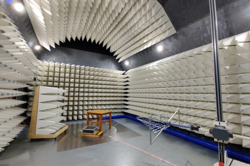
Absolutely. We conduct in-house EMI, ESD, and EMC pre-compliance testing using calibrated labs and spectroanalyzers. This helps you pass CE, FCC, UL certification faster, reducing risk and cost in the electronics product development cycle. See our video EMC test in an anechoic chamber
What is your experience in low-power IoT hardware design?
What is a Battery Fuel Gauge in low-power embedded hardware design?
A Battery Fuel Gauge is a critical power management component in embedded electronics that provides real-time battery state of charge (SoC), capacity, and health. Unlike basic voltage-based monitoring, fuel gauges use advanced algorithms like Coulomb counting or impedance tracking to predict battery life and degradation. In our custom electronics design services, we integrate battery fuel gauges (e.g., TI BQ series, Maxim DS series) into low-power IoT, wearables, and medical devices to ensure accurate runtime estimation, safety, and optimal UX/UI integration for battery indicators. See our video How to Create the Golden Image for Battery Fuel Gauges: Step-by-Step Guide (BQ28Z610DRZR)
Do you offer RF antenna matching and tuning services for custom hardware design?
Yes, as part of our professional RF hardware design services, we provide full antenna matching, impedance tuning, and RF validation for custom PCB designs. Our engineers optimize embedded antennas for wireless protocols such as Bluetooth Low Energy (BLE), Wi-Fi, LoRa, UWB, Zigbee, and NB-IoT. Using tools like vector network analyzers (VNA) and RF simulation software, we ensure impedance matching (typically 50Ω), reduced S11 reflection, and maximum radiation efficiency. Proper antenna tuning is critical for wireless embedded systems to achieve regulatory compliance (FCC, CE), extended battery life, and stable wireless performance. These services are integrated into our hardware development workflows for medical, IoT, and industrial applications. See our video Multi-Frequency Range Impedance Matching for a Single Antenna (Rohde & Schwarz ZNB8 )
Can you provide firmware development alongside custom hardware design services?
Absolutely — as a full-stack hardware and firmware development company, we specialize in delivering integrated electronics design solutions. Our core advantage is the concurrent workflow: our expert embedded software engineers begin firmware development in parallel with early hardware prototypes. This ensures seamless firmware + hardware integration from day one.
This integrated methodology significantly accelerates time-to-market, dramatically reduces development risks, and ensures optimal compatibility across all MCU/MPU platforms, custom PCB layouts, and real-time applications. By acting as a unified hardware design company and firmware development services provider, we eliminate interface ambiguities and debug conflicts. Whether you're building low-power IoT firmware or high-performance embedded systems, we deliver synchronized engineering from schematic to final code, confirming our status as a trusted partner for custom pcb design companies seeking integrated solutions. See our video Hardware product design from an idea to production
Why choose Droid Technologies as your hardware design and custom PCB development partner?
Droid Technologies is a leading European hardware design company with a proven track record in delivering custom electronics development services worldwide. We support clients across the USA, United Kingdom, Germany, France, Sweden, Ireland, Netherlands, Austria, Denmark, Australia, Japan, South Korea, Spain, and beyond. Our team combines expert-level schematic design, custom PCB layout, RF integration, and synchronized firmware + hardware development, enabling fast prototyping and mass-production readiness. We adhere to global quality standards, including ISO 9001, ISO 13485, and IPC-A-610, making us a reliable partner for IoT, medical devices, consumer and industrial electronics.
Do you have client reviews for your hardware and embedded development services?
Yes — we have verified client testimonials and project reviews for our hardware design, custom PCB development, and embedded firmware services. You can find them on:
✅ Clutch
✅ Upwork
✅ YouTube
These reviews confirm our engineering quality, transparent processes, and success in delivering electronics solutions across the USA, UK, Germany, Australia, and other countries.
Do you have a full product development example — hardware, firmware, and mechanical?
Yes — we completed a full-cycle smart blender project, where our team handled the hardware design, firmware development, and mechanical engineering entirely in-house. This showcases our end-to-end capabilities in embedded systems, custom PCB design, and IoT product development. Watch the full case on our YouTube channel to see our process in action. Droid Technologies is trusted by clients from the USA, United Kingdom, Germany, France, Sweden, Ireland, Netherlands, Austria, Denmark, Australia, Japan, South Korea, Spain, and many other countries.
Do you design electronics for regulated industries like medical devices?
Our Offices

Kyiv
Ukraine, Kyiv City, Beresteiska Ave, 67

Vinnytsia
Ukraine, Vinnytsia City, Kyivska 41

Kharkiv
Ukraine, Kharkiv City, St. Karazyna 1,
Kyiv
Vinnytsia
Kharkiv

Kyiv
Vinnytsia
Kharkiv
What can we do for you?

Feel free to get in touch

+380442374050
Ready to request a quote?

Describe your project
Ask for advice from our experts right now
Want to learn more? Need some help with product development? Tell us about your business needs. We will find the perfect solution


