


Hardware / Electronics Design
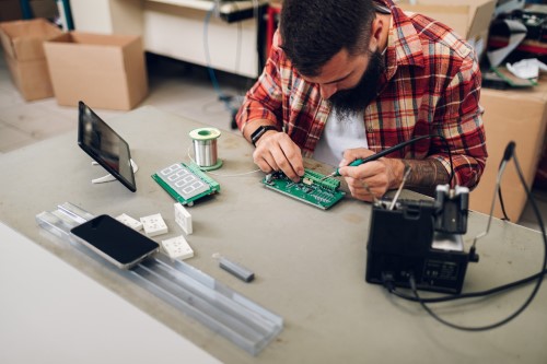
Before each device is ready to use, it must go through some steps, one of the most important is a finished, tested and fully functional PCB/FPC that follows IPC standards
ContactKey capabilities
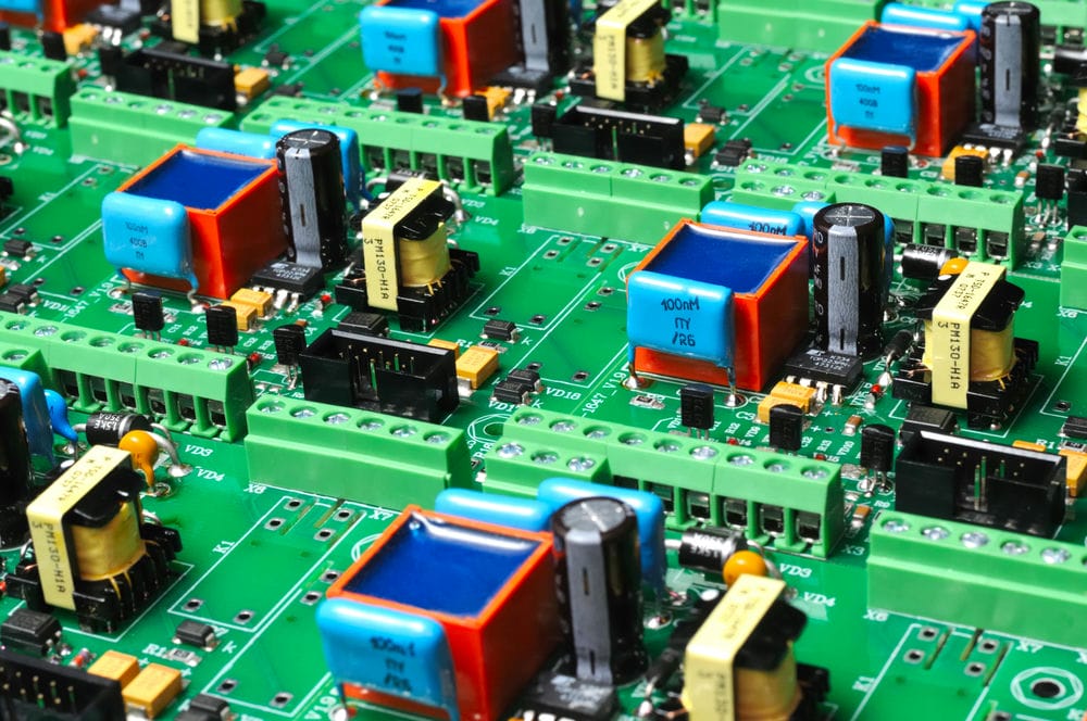
Power electronics design
- PFC - Solar charging controller - Chargers - High voltage control - Motor controllers DC/AC/BLDC
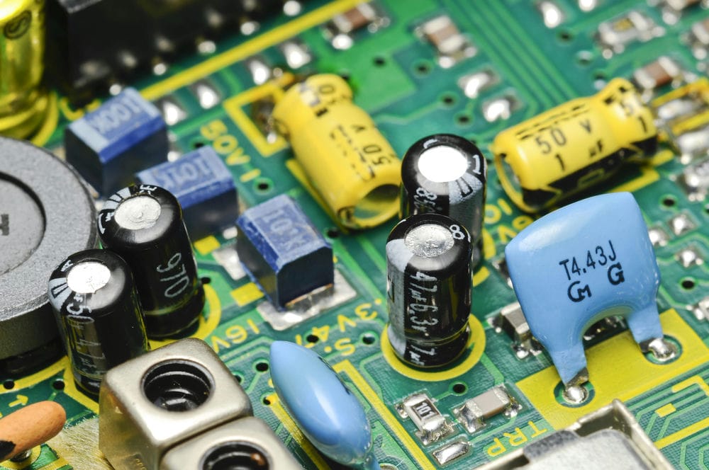
Analog electronics design
- High-accuracy analog measurements (EEG, ECG, PPG, EMG, Piezoelectric signals) - Noise filtration - Digital to analog conversion - Amplifying signal - Analog video CVBS, Analog HD (AHD) - Ultrasound measurements
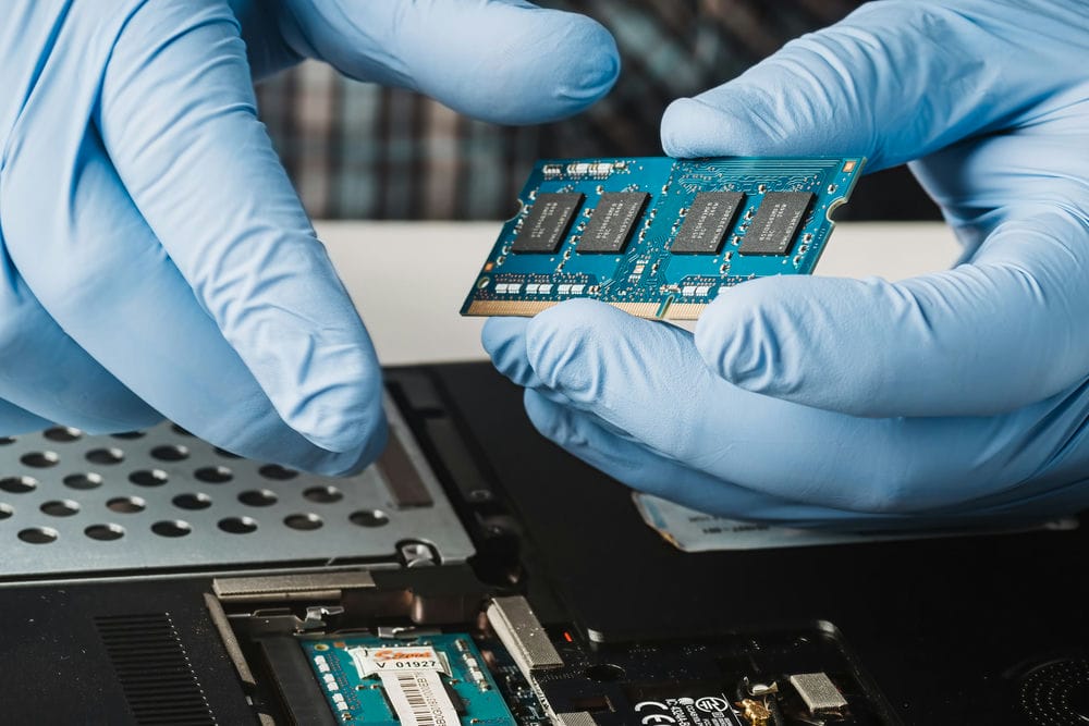
Digital and high speed electronics design
- Memories DDRx/LPDDRx, SDRAM - Camera and display interfaces (MIPI-DSI, MIPI-CSI, DisplayPort, etc) - Data communication interfaces (QSpi, SPI, Uart, I2C, FMC, I2S, USB 2/3.x, etc)
-min.jpg)
RF Designs
- 50-60 GHz (Radars) - 1-6 GHz (UWB, Wifi, BLE, ZigBee, GPS, NB-IoT, LTE-M/LTE, Z-Wave, etc) - 13,6 MHz, 128 kHz (NFC, RFID, etc) - 400-1000 MHz (LoRa, LoRaWan, UHF/RFID RAIN, etc)
Tools that we use
.png)
Altium designer

LTspice
NFC Antenna Design Hub

QUCS

Wcalc

Micro-Cap
Project process
Requirements design
As a first step our team makes technical requirements. After this, we select all the main components, agree on basic concepts with the customer and make a block diagram

Schematic design
Our engineer(s) makes schematic design based on the selected components and technical requirements
Schematic design review
The engineer sends the designed schematic to the reviewer (a hardware developer, that does a schematic review). The reviewer makes a report (use our standard template with a checklist) and sends it back to the first engineer to make corrections
PCB layout
Printed circuit board (PCB) design brings electronic circuits to life. Our engineer(s) makes a PCB layout design that combines component placement and routing to define electrical connectivity on a manufactured circuit board using layout software
PCB layout review
The engineer sends the PCB files to a reviewer. The reviewer makes a report (use our standard template with a checklist) and sends to the first engineer back to make corrections
Manufacturing
Our team creates a bill of materials (BOM) that contains a list of the materials, components, parts, and those quantities needed to manufacture prototypes. After we order components(the USA, EU and China) and PCBs. We assemble samples in our labs(usually 4-6 units) or order them from China/EU/Taiwan/The USA
Device Bring Up and testing
Our engineer(s) verifies the signals, antenna matching (if it has an RF part), loads test firmware, and runs a test (power management, power distribution, checks all signals). If there are any issues in current version, the engineer fixes them by soldering some additional components or wires (find ideally all issues and fix the solution in the Alpha version)
Make Errata document
Our engineer(s) makes one important document that has a list of issues with a detailed description. It needs to fix the schematic and PCB in the next revision
Schematic design modifications
Based on Errata document our engineer fix the schematic
Schematic design modifications review
Our engineer sends out the updated schematic for review, the reviewer checks: the Errata document, the updated schematic and makes the review report and sends it to the first engineer to fix issues
PCB layout modifications
Based on Errata document our engineer fixes the PCB
PCB layout modifications review
Our engineer sends out the updated PCB for review, the reviewer checks: the Errata document, the updated PCB and makes the review report and sends it to the first engineer to fix issues
Manufacturing
Updates BOM, order components, assembles samples (similar steps to the Alpha version
Device Bring Up and testing
Our engineer(s) verifies the signals, antenna matching (if it has an RF part), loads test Firmware, and runs a test (similar steps to the Alpha version)
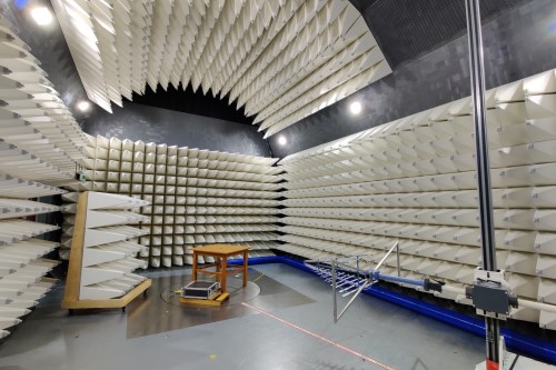
EMC and precertification testing
At this stage, we check our device and do pre-testing in our laboratory, use the spectroanalyzer up to 24 GHz with different antennas and get the first result of the testing. If there are any issues with parasite harmonics, we try to fix them in our lab until it works. As we get everything working we rent a certificated laboratory for EMC and run tests
Make Errata document
We update the Errata document if have issues
Schematic design modifications
Based on Errata document our engineer fixes the schematic
Schematic design modifications review
Our engineer sends out the updated schematic for review, the reviewer checks: the Errata document, the updated schematic and makes a review report and sends it to the first engineer to fix issues
PCB layout modifications
Based on Errata document our engineer fixes the PCB
PCB layout modifications review
Our engineer sends out the updated PCB for review, the reviewer checks: the Errata document, the updated PCB and makes a review report and sends it to the first engineer to fix issues
Manufacturing
Update BOM, order components, and assemble samples (similar steps to the Alpha/Beta version)
Device Bring Up and testing
Our engineer(s) does verification of the signals, antenna matching (if have an RF part), loads a test Firmware, do tests and etch (similar steps to the Alpha/Beta version)
EMC and precertification testing
We rent a certificated laboratory for EMC and run tests
Run pilot
Manufacture 20-50 samples for field testing
Our Offices

Kyiv
Ukraine, Kyiv City, str Vaclav Havel 4, office 422

Vinnytsia
Ukraine, Vinnytsia City, Kyivska 41

Kharkiv
Ukraine, Kharkiv City, St. Karazyna 1,
Kyiv
Vinnytsia
Kharkiv

Kyiv
Vinnytsia
Kharkiv
What can we do for you?

Feel free to get in touch

+380442374050
Ready to request a quote?

Describe your project
Ask for advice from our experts right now
Want to learn more? Need some help with product development? Tell us about your business needs. We will find the perfect solution


